
Snubber Circuit Design Calculators
Driving inductive loads with transistor switches, whether they be flyback transformers, relays or motors often result in the high voltage resonant spikes when the coils are interrupted from their current current source by the transistor. There are various ways of mitigating these undesirable spikes which cause component failures and EMI issues. The most common approach is to use snubber circuits. This engineering tutorial article not only explains common snubber circuits but provides several design calculators, that make snubber design easy.
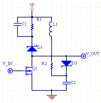
Figure 1 - Coil driving circuit showing the use of a RCD clamping snubber (D1,C1,R1) and a RCD rate of voltage rise snubber (D2,R2,C2)
Method 1 - RCD Rate of Voltage Rise Snubber Circuit
With this method we want to limit the rise of the voltage when the transistor switch is shut off.
Another way of stating the problem is that we want the drain or collector of the transistor to snap back to the rail voltage in dt seconds.
When the transistor shuts off the current is at it's peak value. We can use the following equation to find the necessary capacitance to limit the rise time to a given value.
Ipk= C*dV/dt
C= Ipk*dt/Vrail
We want to only affect the leading edge of the rising voltage and so the time constant (TC) of the RC element must be a fraction of the period. We use the time constant formula for choosing R.
RC= TC
A rule of thumb is to choose Tc to be 1/10th the switch on time.
R= TC/(C*10)= 1/(f*C*2*10)= 1/(f*C*20)
Energy stored in the capacitor is fully dissipated on each cycle through the resistor, so the power that the resistor must dissipate is:
P= Ec*f= (1/2*C*V2)*f
When determining the values of the rise time snubber components empirically there are several relationships that can be exploited.
- With all components fixed and lowering the resistance value, the rise time will decrease and the resistor will consume less power.
- With all components fixed and raising the capacitance, the rise time will increase and the resistor will consume more power.
- Changing the rise time will affect an adjacent clamping snubber. If the rise time increases it will take energy away from the clamping snubber, and likewise if the rise time decreases it will add to the energy that the clamping snubber must remove from the circuit.
Here are some other tips:
- Make sure that the diode can handle the peak current.
- Reduce the capacitor if the resistor is getting too hot.
- Make sure all of the components can handle the peak voltages.
Method 2 - RCD Clamping Snubber Circuit
The clamping snubber is essentially a peak detector circuit used for AM demodulation consisting parallel cap and resistor which is fed by a rectifier. The RC filter is designed to tract the envelope of the AM wave. In this case where the switching frequency is normally constant, the RC circuit will have a ripple induced by the peak inductor current. The voltage can be clamped to a desired maximum dV value by selecting an appropriate valued capacitor. The purpose of the resistor is to fully dissipate the charge on the capacitor each cycle.
This circuit is often found in power supply circuits and they are used to clip the ringing that occurs because of the resonance of the leakage inductance with the output capacitance of the transistor. MOSFETs often have a maximum drain to source voltage which should not be exceeded. The clamp can be designed so that this maximum voltage is never exceeded. The value of the capacitor can be determined by selecting how much voltage change can occur. This delta V is denoted as dV, and can be considered a ripple voltage. We look at the energy flowing out of the coil into the capacitor, and find that the initial energy of the capacitor plus the inductor energy is equal to the fully charged capacitor:
EC0 +EL= ECT
1/2*C*V2+1/2*L*I2= 1/2*C*(V+dV)2
In this case I is the peak current of the inductor, and V is the lowest voltage seen on the RC circuit. Solving for C:
C= L*I2/(dv(dv+2V))
R is chosen such that the time constant is long relative to the period; a time constant of 10 times the period of the switching frequency would be a good choice.
R= 10/(f*C)
The power is equal to the energy from the inductor dissipated into the resistor each second.
P= F/2*L*I2
Follow these tips when fine tuning the clamping snubber:
- The diode selection is critical, make sure that the diode can handle a voltage greater than any of the spikes in the circuit, and that it can handle the peak current. It's better to over-specify this one component from the start.
- Monitor the voltage between the diode and the resistor and cap. This should be a nearly DC value. If it is choppy then either the capacitor is to small, or the diode has too low of a voltage rating.
- There is a trade off between the clamp voltage and the power that the circuit dissipates. The lower the snubber voltage, the hotter all of the components will get.
- Make sure the capacitor has a high voltage rating. The rating must be greater than the expected clamping voltage.
- Adjust the clamping voltage by raising or lowering the resistance, with all other components fixed.
Method 3 - Non-Dissipative Snubber Circuit
Both of the preceding snubber circuits can dissipate large amounts of power through the corresponding resistors. Not only does this cause inefficiencies, but it creates heat transfer problems, and increases component sizes.
The following non-dissipative snubber in figure 2 is overcomes these problems by storing the leakage voltage spike energy into a capacitor when the transistor shuts off. When the transistor turns on again, energy is poured into a parallel inductor, which resonates with the storage capacitor.
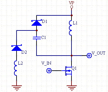
Figure 2 - Non-dissipative snubber circuit. Energy is stored into C1 when the transistor turns off. When Q1 turns on, L2 and C1 form a resonant circuit, and energy that swashes above VP+VD1 is transferred back to the load L1.
The resonant circuit formed by L2 and C1 when Q1 is turned on rings at a frequency of:
F=1/(2*PI*sqrt(L2*C1))
The voltage across L2 will ring negative for the first ring cycle, and then will ring positive for the second. When the voltage across L2 is positive and exceeds VP+ 2*VD all of the leakage energy is transferred back into the supply.
The design steps for selecting component values are simple. First select a capacitor which slows the rise time sufficiently, to lower the overshoot.Selection of the capacitor is by trial and error, since the magnitude of the leakage inductance isn't usually known before hand. After selecting C1, select an inductor such that the two cycle ring period is less than the minimum on time of the transistor - Ton.
L1= Ton(min)2/(4*PI2C1)
References
Abraham I. Pressman, Switching Power Supply Design, , ISBN 0-07-052236-7